


|
Thin Film Silicon – Higher Efficiency and Lower Costs
A new generation of thin film silicon technology is regaining cost and performance leadership with key innovations helping to drive down cost and increase energy output and reliability to make solar power competitive. Cost reduction is the key objective of the photovoltaics (PV) industry as it strives to position solar power as a low-cost choice for new energy capacity.
Three years ago, silicon wafer prices were high and PV modules were in short supply. With crystalline silicon cells making up ~80% of the PV energy capacity produced annually, fluctuations in supply and cost of polysilicon in recent years created a window of opportunity for thin film technology innovation, driven by manufacturing equipment suppliers seeking new high-growth business opportunities and by module manufacturers looking for ways to diversify and/or enter a fast-growing world PV market. Within a short period, many existing and new PV manufacturers began choosing thin-film silicon technology to reduce their strategic dependence on polycrystalline silicon and to capitalize on new innovations in thin film technologies promising an advantageous manufacturing cost. Then the world PV market changed in 2009. Today, silicon wafers and PV modules are in more ample supply, and negotiating power has shifted back to the buyer, though the near term outlook for c-Si components is somewhat uncertain because of accelerating demand. With cost leadership now a matter of survival in a tight PV market, the competitiveness of thin-film technologies has been challenged. However, a new generation of thin-film silicon technology is poised to regain cost leadership within the industry. Key innovations are helping to drive down cost and increase efficiency and reliability to reinforce thin film's competitive advantages in end user markets.
The fundamental advantages of thin-film silicon have not changed. Thin-film silicon PV modules require far less silicon than traditional methods (less than 1/100th of a wafer thickness) and use widely available, comparatively inexpensive materials. Thin-film silicon technology is inherently suitable for achieving very low manufacturing cost because the entire manufacturing process from bare glass to a complete PV module requires significantly fewer manufacturing steps than conventional crystalline technologies. Another key positive factor is that thin-film silicon technology uses only environmentally friendly, non-toxic substances. Finally, thin film silicon panels have an inherent advantage in real energy performance, due primarily to the fact that thin-film silicon has a temperature coefficient "penalty" that is almost 50% lower than most conventional crystalline. In hot climates, this advantage results in 5% to10% higher output per installed watt compared to crystalline silicon.
Oerlikon recently announced that their Thin Fab manufacturing line design has improved productivity, reducing the expected cost of production to €0.50/Wp and at the same time, a 100% increase in the output capacity and a 50% reduction in the CAPEX per Watt. Together with improved stabilized lab cell efficiency of 11.9% (world record for thin film silicon) Micromorph technology enables the production of PV modules with a 10% stabilized module efficiency (roughly equivalent with First Solar) – but at even lower manufacturing costs (by a slight margin). These achievements are the result of innovations in cell and module design, equipment and facilities, silicon and TCO depositions, laser tools, and materials. Each of these is discussed below.
The efficiency of Micromorph cells and modules is the result of a combination of interrelated design innovations that significantly lower manufacturing costs. Improved transparent conductive oxide glass-coating (TCO) increases the transmissivity of the front glass and also enhances light scattering, increasing light capture (Fig. 1). 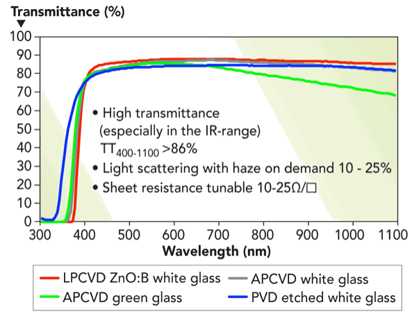
Thinner amorphous and microcrystalline silicon "absorber layers" increase stabilized efficiency while reducing material costs and increasing manufacturing throughput. Finally, a new highly reflective white lamination foil enhances light capture and efficiency by reflecting photons back into the absorber layers of the cell. 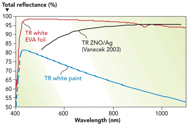
Figure 2 illustrates the improvement in reflectance that is achieved by using a white lamination foil instead of a layer of white paint. The introduction of a white lamination foil also helped to accelerate manufacturing productivity, as previously two manufacturing steps (applying white paint, then adding a transparent lamination foil) were replaced by one simpler manufacturing step (applying a white lamination foil). The combined effect of all of these improvements is a dramatically lowered production cost, now estimated to be €0.50/W with the new equipment. Also, the capital expenditure for Watt-peak power (Wp) is significantly reduced, largely as a result of increased equipment productivity. Finally, these changes have improved module performance with the new design yielding an expected production average module efficiency of 10% (stabilized). This new efficiency standard for thin film silicon will result in additional cost savings for installed PV systems.
In addition to cell and module improvements, new advances in manufacturing equipment and manufacturing processes also play a critical role in reducing the cost of thin film silicon technology. Over the past year there has been significant progress in accelerating throughput and increasing expected reliability and yield for several key manufacturing tools used in the production of Micromorph thin film silicon panels.
A new design for silicon-deposition PECVD tool, the KAI MT, was announced earlier in 2010. This tool builds on a well-proven design, including a high-frequency 40MHz Plasmabox reactor design that enables comparatively faster and uniform silicon deposition. The new design incorporates two significant changes that result in increased capacity and reduced footprint. First, the new design incorporates three deposition chambers per tool, with each deposition chamber capable of handling 10 modules at a time. The new configuration can be seen in Fig. 3a, where "PM" refers to deposition chambers. Previously, the KAI had just two deposition chambers per tool. This new design provides a 50% increased glass coating area and throughput, with no significant increase in equipment cost. Productivity is further enhanced by a modification in the silicon deposition itself, whereby both the a-Si top cell and the microcrystalline bottom cell are deposited in the same chamber, eliminating the need to expose the glass to atmosphere in between deposition processes and improving overall deposition speed and quality. Secondly, the configuration of the deposition tools has been made significantly more compact by shifting the location of auxiliary equipment (e.g. vacuum pumps) to a mezzanine above the system, resulting in a 50% reduction in footprint.
Another example of significant equipment performance and production cost improvements is seen with the equipment used for deposition of transparent conducting oxide (TCO). This deposition is done in a low-pressure chemical vapor deposition (LPCVD) process and toolset. The integration of this TCO deposition tool into the thin film silicon manufacturing process allows for two key advantages over the use of pre-coated glass. First, on-site TCO deposition allows for the use of zinc oxide (ZnO) for the TCO layer, a material that yields a significantly higher performance than commercially-coated glass (which uses tin-oxide). Second, including the TCO deposition tool in the thin film silicon manufacturing line allows for optimization of the interface between the TCO and silicon absorber layers, resulting in enhanced light scattering, which results in increased light capture and higher module efficiency. Furthermore, the integration of TCO deposition into the thin film silicon manufacturing line allows manufacturers to use plain uncoated glass as a feedstock, resulting in a cost savings of €10 per panel or more compared with the cost of using pre-coated glass. The most current version of the TCO deposition tool, incorporates several significant improvements. For example, optimized shields allow significantly stretched cleaning intervals. the deposition rate has been improved substantially' and the back transport of the glass has been changed for easier maintenance. As a result, the tool achieves higher uptime and throughput in the field.
The third example of "core" manufacturing equipment used in the production of thin-film silicon PV modules is the laser tool, used to sculpt the thin-film silicon and TCO layer stacks to form interconnected PV cells. Two key laser performance parameters that help to drive down production cost are the laser accuracy and the laser tool's processing speed / throughout. Improved laser accuracy results in a reduced "dead zone" between cells resulting from laser scribes. 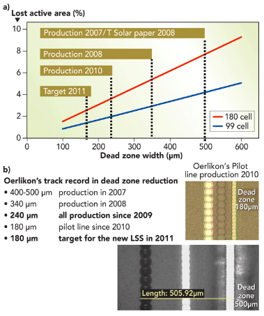
The laser tools included in this manufacturing line are now capable of producing Micromorph modules with roughly half of the dead zone thickness that was typical for production just two years ago (and that is still typical for many thin-film module manufacturers today). The result is a reduction in the area loss within the module and higher module power. Furthermore, the newest laser tool (LSS) has doubled the number of laser heads, resulting in a 100% increase in throughput compared with previous generation tools, with increased reliability and uptime. In sum, the changes outlined above to the "core" manufacturing equipment tools have resulted in thin film silicon modules with substantially increased performance and productivity with: 1) a more than 50% throughput increase,
In thin film silicon manufacturing, materials (e.g., glass, lamination foil, junction box, etc.) represent over 50% of the total cost of a thin-film silicon PV module. Reduction in the amount and price of key materials is a major factor in driving down the total cost of module production. Technology providers can greatly reduce the expected cost of module manufacturing by optimizing the design of the module itself, while aggressively working with suppliers of key materials to qualify several competing vendors of key materials for the modules. Oerlikon has achieved a 50% reduction of material cost over the last three years, thanks in part to qualification of new suppliers and optimizing the minimum requirement specifications. In addition to the white lamination foil example described above, other significant material cost reductions have been achieved in the junction box, contacts, encapsulants, and the front glass. Thin film manufacturing equipment leaders are demonstrating tremendous potential to accelerate the pace of PV performance improvements and cost reductions, helping to position thin film silicon PV manufacturers to be competitive with other PV industry cost leaders, helping to make solar power economically viable.
Micromorph and Plasmabox are trademarks of Oerlikon Solar. Photos and illustrations were first posted at Renewable Energy World.com
To find related articles - use our built-in / Google Powered site searching tool below. Just type in a few key words or phrases to search this site, our blogs, our Facebook fan page and other sites for related articles.  Custom Search
|